Forlab PICT2DES
The use of ultra-thin, two-dimensional materials in electronics and sensor technology enables completely new types of transparent, flexible and biocompatible solutions with minimal resource consumption. However, the technology for this promising area of microelectronics has not yet reached the level of maturity required for industrial applications. The Bochum Microelectronics Research Laboratory for 2D Electronics aims to change this. Martin Hoffmann at the Ruhr University Bochum are working on establishing a stable process that integrates additive and subtractive technologies with high yields at wafer level, which will allow a transfer to industry.
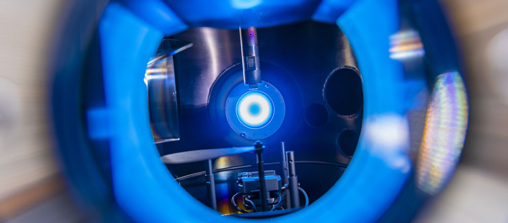
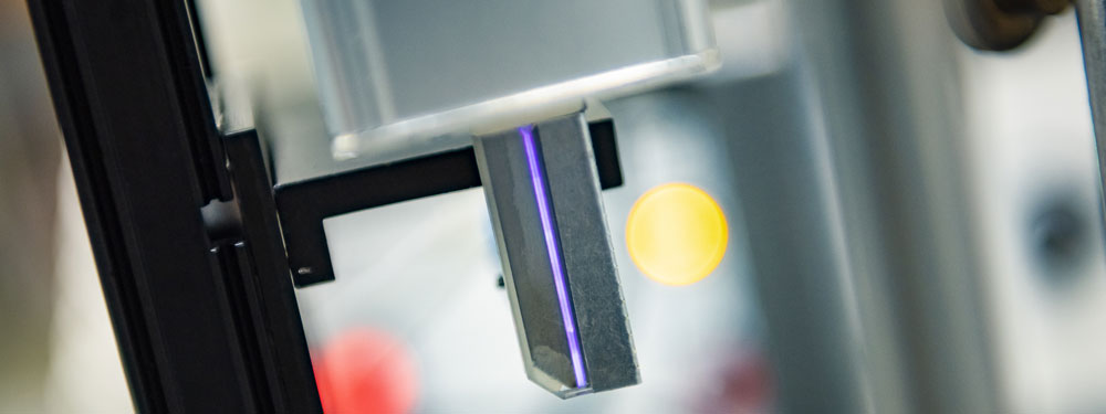
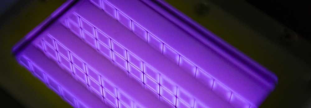
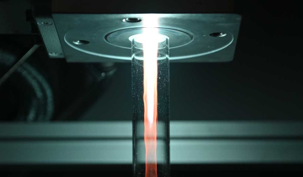
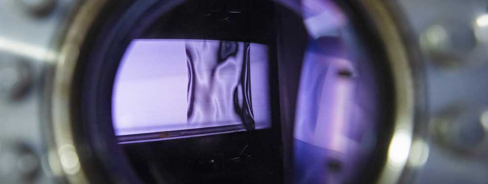
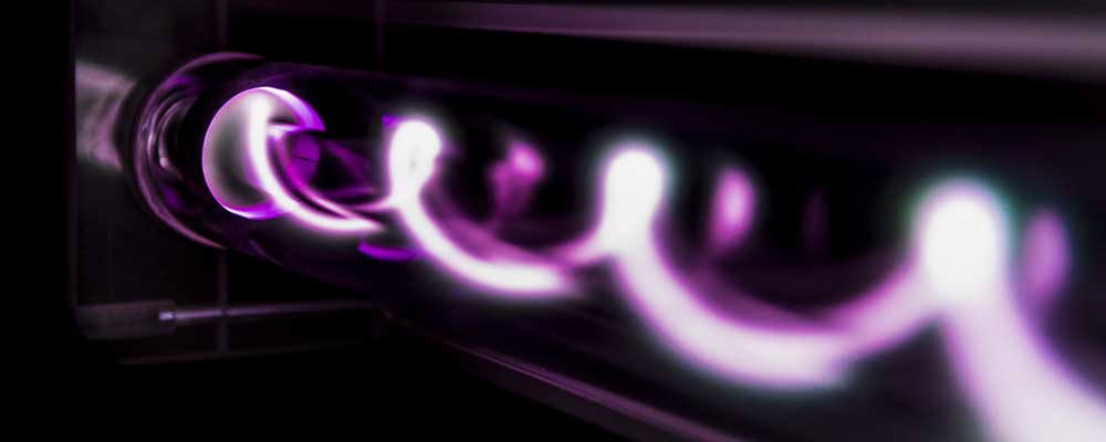
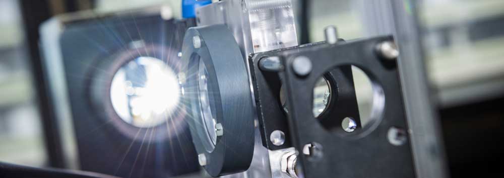
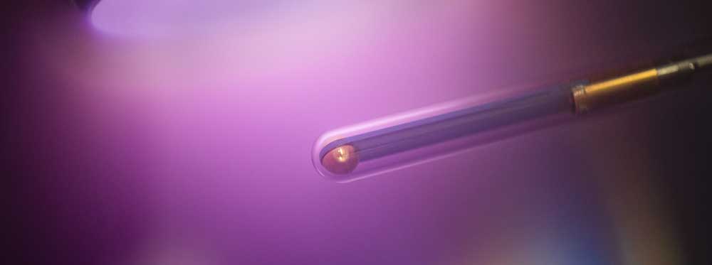
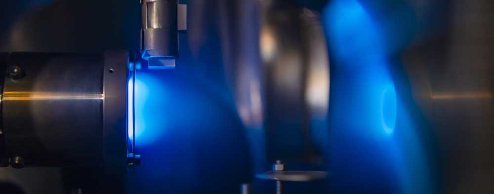
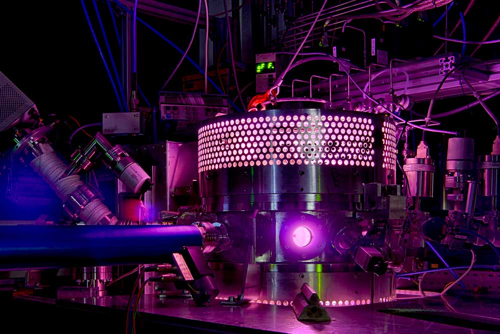
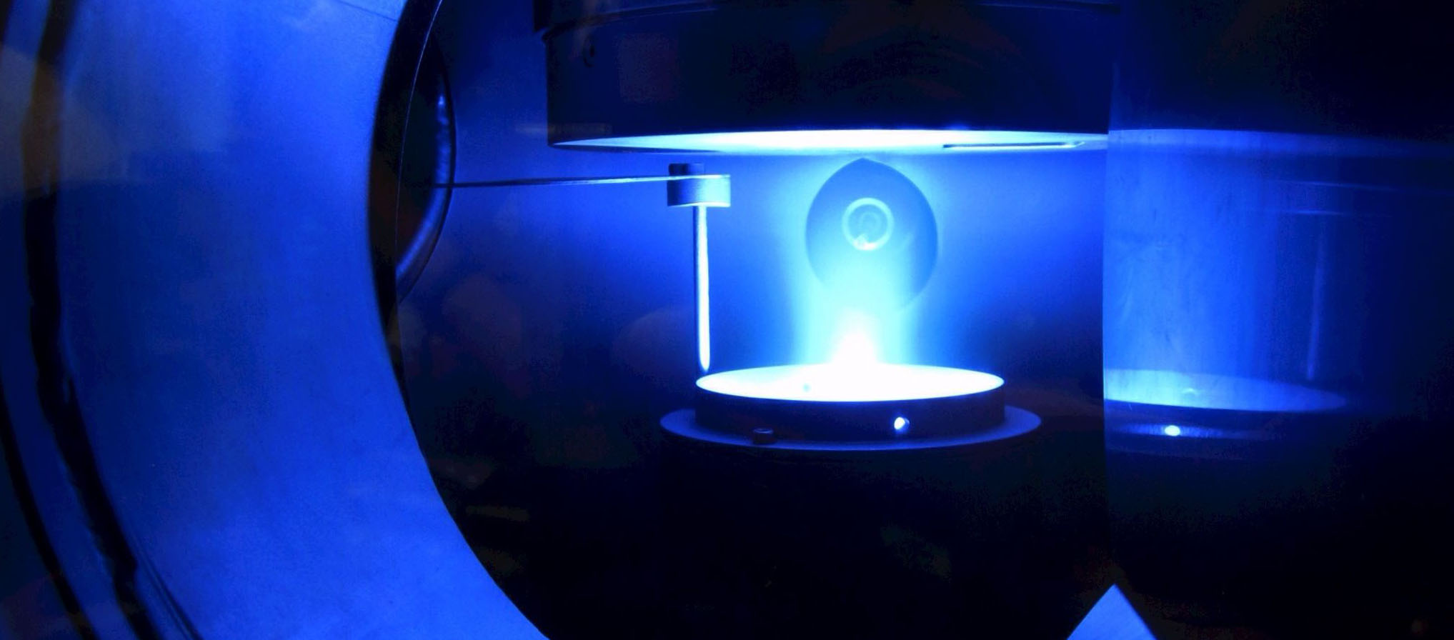
They are focusing on the entire process chain - from the raw materials, the so-called precursors, to the high-precision generation of ultra-thin layers by atomic layer deposition, to structuring with novel selective and low-damage plasma etching processes for the defined exposure of individual ultra-thin layers.
In the project, an innovative, monolayer-accurate deposition and etching technology at low temperatures for the production of low-cost, flexible microelectronics and ultrasensitive microsensor technology is being developed and implemented in a 200 mm cluster system on substrates compatible with the Forschungsfabrik Mikroelektronik Deutschland and industrial users.
The aim is to develop novel, particularly resource-efficient electronic systems based on 2D integration. These include flexible microelectronics, highly sensitive sensors as well as microfluidic systems for medical technology and energy conversion and autonomous sensor arrays.
Contact
Prof. Dr.-Ing. Martin Hoffmann
Chair of Microsystems Engineering
Faculty of Electrical Engineering and Information Technology
Ruhr University Bochum
Further information
- Website SBF 1316 https://www.forlab.tech/ueber-forlab/forlab-pict2des/