Defect diagnostics
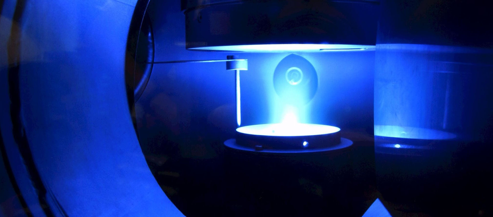
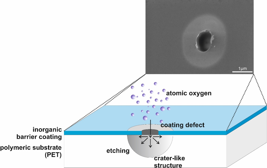 In the field of encapsulation of microelectronics or packaging industry the application of plastics is wide spread, due to their cost efficiency and easy processing. Especially, in packaging industry polyethylene terephthalate (PET) and polypropylene are the dominating material. Nevertheless, plastics offer only limited barrier performance against permeation of gases, e.g. oxygen or CO2. A significant increase of barrier performance can be achieved by the deposition of thin inorganic films by means plasma processes. However, these kind of plasma coatings contain microscopic defects which limit the resulting barrier performance. Usually, these kind of defects are not visible with optical or electron microscopy. Hence, visualization of defects is applied by reactive oxygen etching. This is based on etching the polymer surface underneath coating defects by reactive oxygen species and subsequent imaging with SEM. Most organic polymers like PET are sensitive towards etching by reactive oxygen species. In contrast to this, most inorganic materials like SiOx and TiO2 are almost chemically inert with respect to reactive oxygen species and therefore, etch rates are typically below detection limit. Hence, the inorganic barrier coating serves as a mask against etching and protects the polymer beneath. Nevertheless, reactive oxygen species like atomic oxygen can enter defects and etch the unmasked polymer surface at defect sites. Due to scattering of atomic oxygen in the gas phase etching occurs nearly isotropic, resulting in undercutting of the barrier coating. Subsequently, a crater-like structure is formed. In SEM images, this structure appears as a dark spot in the center surrounded by a whitish circular ring. The dark spot represents the defect, i.e. hole in the barrier film. The number of defects and associated defect density are then determined by an automatized image recognition software, based on the image processing toolbox in MATLAB.
